Hello everyone. My name is Muhammad Haris Rais. I am a PhD student at SAFE lab – Security And Forensics Engineering lab at Virginia Commonwealth University. The lab is led by Dr. Irfan Ahmed and is mostly focused around industrial cybersecurity, and its forensics.
Today, I’m presenting a hardware based PLC memory acquisition framework called Kyros. And in this work, we are collaborating with Rima Asmar Awad and Dr Juan Lopez Jr from Oakridge National Lab.
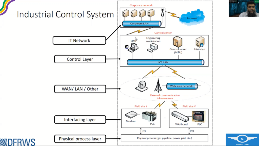
An Industrial Control System is a collection of devices, a variety of network and control software, to basically operate or automate a physical process. A physical process could be a gas pipeline, power grid, a nuclear power plant, water treatment, any other.
And these physical or field devices, they actually interact with the physical process to connect it to the cyber world, and field devices themselves are connected to a variety of networks, to a control center that hosts different controls, software – engineering software, and HMI. And this control center is connected to corporate LANS, which are typically connected to internet.
If we see the uniqueness of this industrial control system, it lies in the, this interfacing layer, where we have these field devices, which are most commonly programmable logic controllers or PLCs.
A PLC is a rugged industry specs embedded system. It has a CPU volatile/non-volatile memory component and optionally, some removable storage, and a host of input and output modules to connect to the physical process.
The control application running on the firmware in the PLC is usually called control logic program and PLC executes a loop, a continuous loop in which it gets the state, current state of the system through the sensors, and then applies some control logic over that state, and calculates new output values that are applied to the actuators where they tend to steer the physical process to a new state, and then began the new state of the system, and the loop continues.
If you talk of memory forensics of PLCs, there are two distinct research areas in memory forensics. One is the acquisition of memory and another is the analysis of memory. As far as acquisition of PLC memory is concerned, so far the research is mostly focused on the software tools like debugging tools or ICS protocols, or maybe analyzing the network data.
But if we have the physical access of the device available, so why not to explore the hardware based approach? JTAG interface is explored in the past as well, but only for modifying PLC firmware. So far, there is no work or framework that guides a forensic investigator on the process of extracting memory, complete memory of a PLC through JTAG.
A little bit on the JTAG. In 1980s, when ICs were shrinking and circuit boards were getting more and more complex, so the testing of the circuits became difficult with the existing approaches. For example, if you see this IC, it’s a ball grid array design, where the contacts are not on the sides, rather on the bottom of the IC.
And when we put this IC on a circuit board and solder it, and if there are some errors, like if you see it from the side view, if there is an open circuit, or there are some short circuits, so with conventional approach it is very difficult to find these types of errors.
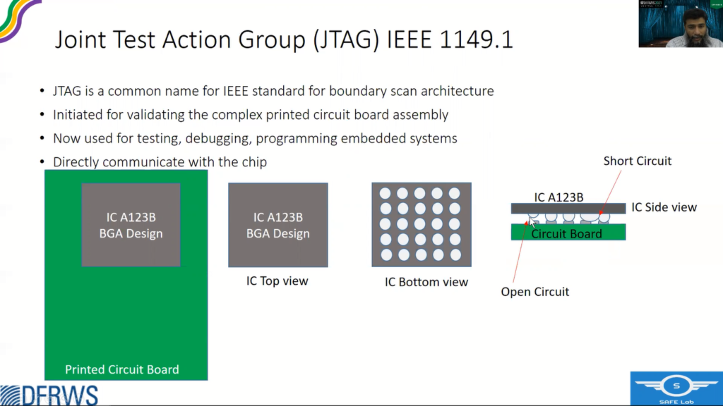
Then the vendors sat together and came up with an idea of including some kind of circuitry within the chip that should facilitate the testing. And later this was standardized by IEEE as IEEE 1149.1. for boundary scan architecture.
If you see this is a normal IC package, where the core circuitry, comprising of target cells and gates, they are connected to the outside pins of the IC. In JTAG, there is a boundary scan, serial register or shift register that is, that sits between the core circuitry and the pins.
And there is a TAP Controller, which is a smart state machine that can control these registers and through these registers, a user can control the output going out of the pins, or can also read the input that is coming into a particular pin, and that’s how it facilitates circuit testing. But later on this approach was also utilized for debugging and embedded system programming also.
Kyros framework constitutes two phases.
In the first phase we create a memory profile using a test PLC, and in the second phase, we use that profile to acquire the memory of a suspect PLC.
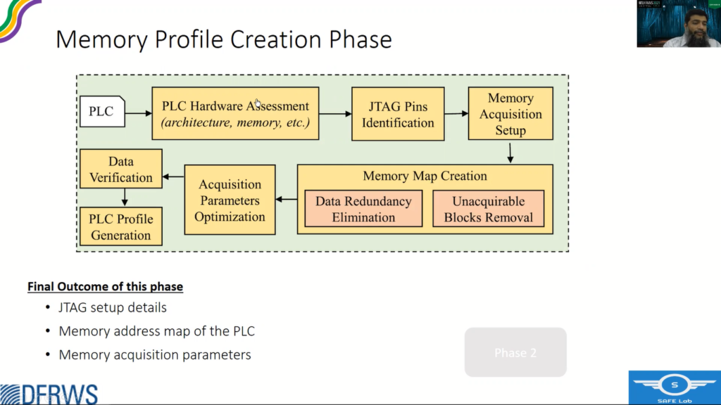
So in phase one, the first step is Hardware Assessment. So while analyzing the hardware of a PLC we are mostly interested in the microcontroller, the architecture of the microcontroller and its internal memory and volatile, and non-volatile memory components, the JTAG pins of the microcontroller and the memory address map, like where the flash resides and where the RAM resides, what are the peripheral addresses and so on.
The other components are the memory elements that are available in most circuit boards because the internal memory of a microcontroller is not sufficient, so there are external memory components as well, like volatile memory components or non-volatile memory components, and then the removable storage, which is also not part of the memory, but it facilitates in verification of the memory content that we require.
The main sources of information for hardware assessment.
The first one is the PLC hardware manuals, although they don’t specify a lot of details, but there are some hints like, well, how much is the Code memory or the IO memory or controller architecture and the backup options available or not? So they give a hint of what type of, how much is the memory that is available.
Next is the visual inspection by disassembling. So we disassemble the PLC and see the boards. There could be like four types of boards, communication, main board, power, but we are interested in the main boards, and we examine the ICS that are available on the circuit board.
And again, we are looking at the controller IC and the memory elements IC. Once you find the IC there, hopefully there are part numbers, then we search the data sheets and find out the details of the memory, like how much is the capacity of the memory and what are the different parameters, what’s the type of memory and so on.
So the next step is to identify the JTAG pins from the Processor Datasheet. If the Processor Datasheet is available, it clearly tells us which pin is the JTAG pin, mode selector or input output pins.
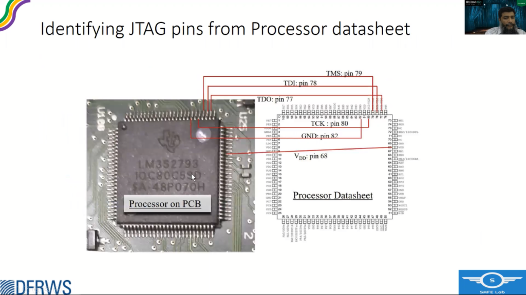
So what we can do, if we have those available, we can clearly see on the processor IC where those pins are located, and once we do that, the next step is to identify the JTAG contact pad, although like, we identify the pin on the processor, but it is very risky to use these pins for extracting information or controlling the TAP controller.
So even the vendors, they use a pad, contact pad through which they control the TAP controllers. And once the circuit testing is completed, they usually remove the connector on that pad, but we can still find that contact pad available on the circuit board.
So how do we find it? One way is to do connectivity tests through multimeters, or use some heuristics, like what are the pads that are available in the vicinity, empty pads that are available in that vicinity.
So just to quote an example, like there are four different PLC that we were working on, and these are their JTAG contact pads. In one case, it is even labeled like, but in most other cases, there are no Headers installed, and there is no labeling, but it’s still the JTAG. As you can see, it’s very near to the processor.
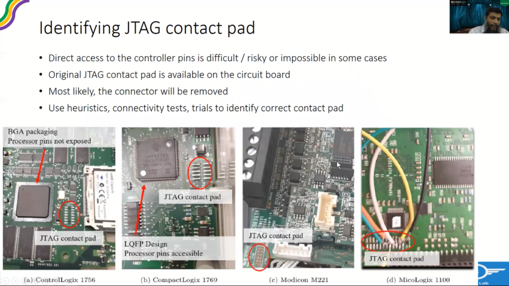
So if the data sheet is available and we know the pins and we see a potential pad, we can do a connectivity test, like through multimeters we can find which of the pins is actually connected to these particular pins of the processor. And then once we identify a contact pad as a JTAG pad, what we do, we install a header on it, solder a header on it, and route the cable out of it, because to use JTAG, we have to power up the PLC, and for that, we have to reassemble the PLC.
So another way is just to solder the wires on the contact pad as we already identified the pins, so instead of going for a complete header, just solder the wires, but this approach is not that robust and it’s risky as well. It’s a small, extra effort actually gives more dividends.
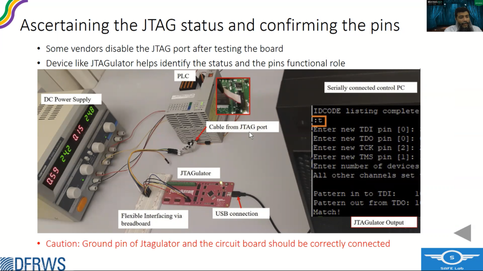
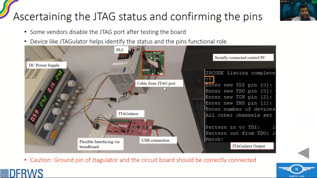
So at times, vendors do disable the JTAG after testing, so we need to ascertain the status of the JTAG. And for that, we use a small device called JTAGULATOR and actually we connect the contact pad that was available on the circuit board to the connector available on the JTAGULATOR and what it does it do all sorts of combinations and permutations to find out the exact pins, JTAG pins. And if it successfully finds out, that also confirms that the JTAG is still functional right.
One caution, that while using JTAGULATOR the ground should match, so you have to manually match the ground before starting the JTAGULATOR.
The next step is our memory acquisition setup.
So once you find the JTAG pins, like how to use a JTAG for memory acquisition? So JTAG has like few pin outs and they, these pins work at the controllers’ operating voltages. So how do, I mean, we need, we would require some voltage converters, then we would also require some BSDL files and then create programs to exploit JTAG for reading memory.
And instead of going through all that hassle, the simpler approach is to use off the shelf JTAG debuggers that have very extensive libraries for the data, for the processors that they support. So like these are some famous debuggers that we can choose after verifying if they support our architecture.
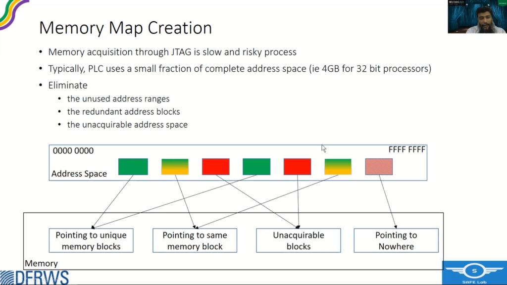
So once the setup is ready, the next step is to create the memory map. So memory acquisition through JTAG is a very slow and risky process. However, fortunately PLCs only use a fraction of the complete address space of the processor. Like for a 32 bit processor of a probable four GB space, usually PLC uses a hundred MB, or even less than that, or a bit more than that.
So if we are able to eliminate the unused spaces, unused address ranges and redundant address blocks, address blocks that point to the same memory location, and the unacquirable addresses, which are pointing to the peripherals. So if we are able to eliminate this, we can actually find out that small fraction, which really helps us in catering for this slow process of JTAG recovery.
Now, if you see here, I mean these are the address ranges that actually point to unique address blocks, and some of the addresses may point to same address blocks. So we are not interested in both of them, or all of them, we are only interested in one of them. If you acquire one, we are good and we don’t need others.
Then there are some address ranges that are pointing to peripherals, which may crash the PLC, and we are not we are not interested in acquiring these address spaces. We have to eliminate that. And then there are other ranges that are pointing to nowhere, and we are not interested in them as well.
So one caution in eliminating the data redundancy. So not all duplicate address blocks are redundant. So this is an important thing. For example, if the firmware is loaded in the non-volatile memory and the volatile memory is in the Ram as well, so these two are considered as two different artifacts from forensic perspective.
So if we just see like these are both the same, so they may be pointing to the same address, these are the same memory, and we just ignore one, that won’t be correct. So what we should do, we should employ some kind of logic like address boundaries. If no unused pins are identified, then we have to keep the copies. And another approach is to write to an address and to see the effect on other copies.
The next step is to eliminate the unacquirable address blocks, which are originally pointing to peripherals and they can crash the PLC. So to identify them in one way is to check the processor data sheets. If they’re not available, then do a ‘Crash and Learn’ exercise, it’s a patient exercise that we have to perform on the test PLC.
And it will crash the PLC, so if we have some kind of software based or device recovery technique, like maybe PLC provides some kind of mechanism to reboot it, or if not, then we can also use power supplies that can be controlled through software. It can really facilitate this ‘Crash and Learn’ exercise to identify unacquirable address blocks.
So the next step is to optimize the acquisition parameters. So as JTAG based acquisition is below the firmware level, it may expire some watchdog timers, resulting in a PLC crash. As a matter of fact optimisation also helps in speeding up the process involved, and it should be performed on a per IC or more specifically per address block basis.
The parameters that we should optimise include like acquisition speed, block size, Debugger’s buffer size, and wait time between consecutive read operations.
And how to find these, the values from these parameters, one way is to theoretically derive them from the processor information, the ICS information like the refresh rates, et cetera, and the debugger specifications.
And the other approach is a practical approach to discover through a ‘ramp up till crash’ approach, like we speed up as we do in DCP that you speed it up until it crashes. So as there are very limited memory regions after the first initial exercise, the second approach is feasible and faster and easier as well.
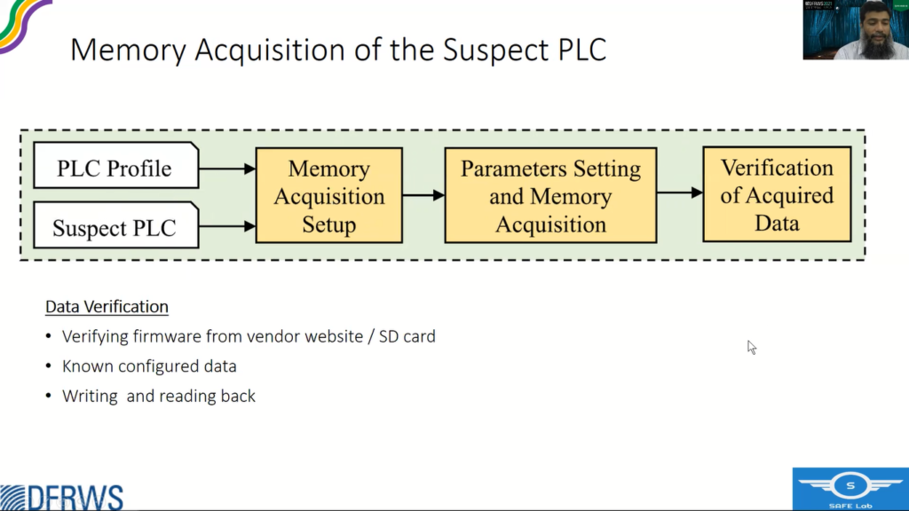
So once we get that memory profile, we do the memory acquisition of the suspect PLC. So instead of test PLC we have the suspect PLC we set up the acquisition mechanism and set the parameters and acquire the memory and do a verification exercise.
For verification, firmware is very helpful. It’s a big file, and we can verify if we are getting the correct data from the, through our mechanism acquisition process.
Other way is to find through the known configured data like the IP addresses and other ASCII characters, for example inventory of the PLC, or maybe the project file name, et cetera.
Third approach is writing and reading back. So you write, through JTAG we can write to the memory content as well. So we write and then read back to verify whether we are writing it right and are reading it correctly or not. So that actually verifies the acquisition process.
Coming over to the case study, we did a case study on a famous Allen-Bradley control logic, 1756, which is a modeler PLC, and it was hosting a controller 1756-L61.
So coming over to the hardware assessment that main controller it’s using is like V Y 2 2 5 7 5, which is an ARM processor that’s written on it, but we were unable to find the data sheet even after contacting the vendor, so it was regretted.
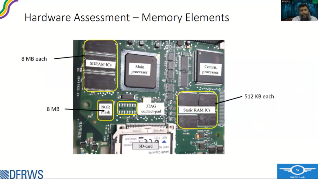
So what we did, so we examined the complete board and that memory contents that are available are static Ram ICs. There are four of them, each with 5, 1, 2 kilobytes, and a NOR Flash, and three SDRAM ICs. There was an SD card as well that can hold like the firmware backup or the program backup.
So to identify the JTAG pins, there was a two by seven big contact pad, which was a potential candidate, and because of the BGA design and no availability of data sheet, we could not do any connectivity testing. So what we did, we installed the header on it, and a cable and routed it out and then used the JTagulator to confirm the JTAG pins and the JTAG working status.
So this is where typical memory acquisitions that we used Segger J-Link debugger for it. And this is the hole that we punctured in the chassis to extract the cable out and connect it to the debugger.
So talking about redundant data. This is an example case, like all these memory addresses are pointing to one single memory location. And if you see here these are the offset, memory offset, and this is like where it is pointing to a particular device. And these are unused pins, i.e. they don’t, or you can say don’t care pins.
So after acquiring the data, we perform on them a Parameter Optimisation exercise as well. So there were only 28 distinct ranges of different sizes. So we applied a ramping up technique instead of going through the theoretical exercise of finding the parameters, parameter values.
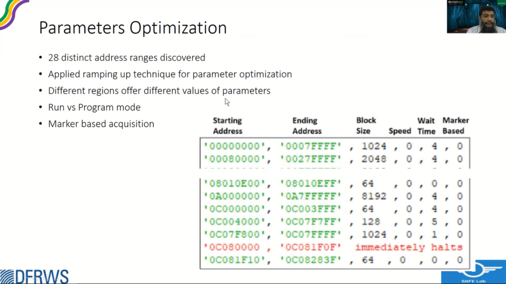
And one more important thing is like, if the PLC is in run mode or the PLC is in program mode, it may respond differently to different acquisition parameters.
The finalized address ranges. Some of them, if you see here this, these three it’s like 16 MB block, and it is repeated like eight times till this particular address. So only acquisition once is sufficient. And then there are some addresses that actually hang the processor, which probably pointing to some peripherals and we should avoid them.
And then if you see here, the data above the six, eight, all zeros was not in use. It was, the data was nil ended until all left. So like more than half of the address space was not utilized.
So Phase Two was the acquisition, memory acquisition of suspect PLC. So we did not have another PLC of the same model, so we used the same test PLC for the next phase.
We programmed, we wrote a small program using a Pylink library that was available for Segger J-Link debugger, and our program can operate in three modes. It can acquire all the complete acquirable memory, or we can provide a customized range to extract that particular memory region. And we can also do signature based acquisition, like if you have some markers available for the start and end of a particular zone, we can acquire that particular memory as well.
So for verification, reasonable confidence was already attained during the profile creation, like when we were identifying the redundant blocks. So what we were doing, we were actually confirming the acquisition correctness as well, because we were matching the different region data.
But we also downloaded the firmware from the vendor’s website and then matched it from the multiple instances that we were getting from available memories, and we perfectly matched them. So we also did an exercise of acquiring data across the memory, all different regions over multiple restarts, and the result was a hundred percent.
Limitations. We need a separate PLC for profile creation, as you can not risk using the suspect PLC. It’s a hardware based acquisition, definitely requires hardware interference, disassembly, soldering, header installation, et cetera. And if the vendor has disabled the JTAG interface, this approach can not work.
In the future we are intending to employ and evaluate the Kyros framework on other PLCs as well.
So to conclude, we presented Kyros framework for hardware based memory acquisition of PLCs. Kyros guides a forensic researcher on how to tackle the hardware challenges related to JTAG and deal with proprietary hardware and customized ICs, with no data sheets, and to generate a memory map and optimize the acquisition parameters. And we also presented a case study of the framework on Allen-Bradley ControlLogix 1756.
Thank you.